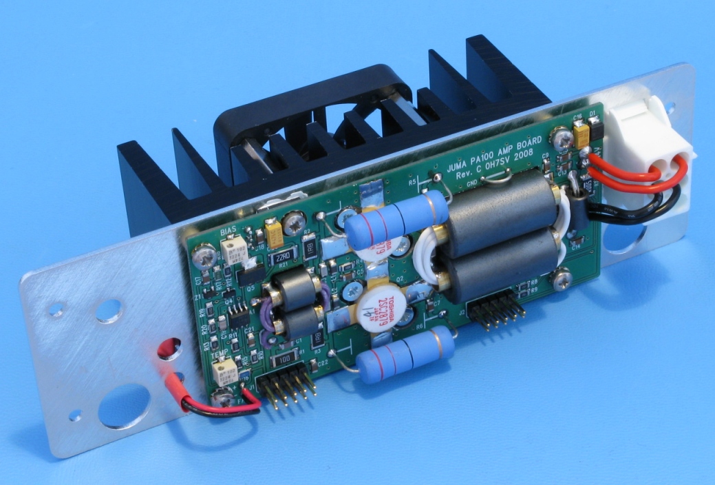
General
The amplifier module provides
the gain for the 100 watt output in all ham bands from 1.8 MHZ...28 MHz.
The amplifier PCB is mounted into the rear panel including the heatsink and
the temperature controlled fan. The nominal supply voltage is 14 VDC and
the maximum current is over 20 A. The DC supply input is protected against
over voltage and reverse polarity with the transil diode D1. The connections
to the other PA100 modules is done with two flat cables. The supply voltage
coming from the DC connector is fed with four soldered wires.
Amplifier circuit
The input transformer T1 transforms
the 50 ohm impedance to the low impedance level for the bipolar RF transistors.
The passive components R1, R2, R3, C1, C3, C4 with the feedback resistors
R5 and R6 provides a frequency correction to achieve a flat frequency response
over the 1.8 MHz...30 MHz range. The bipolar RF power transistors Q1 and Q2
are in working in class AB in push-pull configuration. The output transformer
T2 transforms the low ohmic collector impedance back to 50 ohm level. The
RF transistors are cooled with the heatsink in the rear panel including the
temperature controlled fan.
Current sense
The very low ohmic resistor
R7 is in the current path of the power transistor collector current. This
resistor is a SMD 2512 size and there are four solder pads to achieve a four
wire "Kelvin" connection to the current sensing resistor. The differential
voltage across the resistor is fed to the main board to detect the collector
current. Current reading is further wired to control board for indication
and over current protection.
Bias supply circuit
The bias supply voltage is
referenced to the P/N junction voltage of the transistor Q3 which is installed
to the heatsink. This provides a sufficient negative temperature compensation
for the final transistors. The bias adjustment is done with the trimmer resistor
R18. During transmission the bias voltage is connected to the final transistors
with the MOSFET Q4. The bias voltage is buffered with the OPAMP A1-A and the
transistor Q5 and fed to the base via the inductors L1 and L2.
Temperature sensing circuit
The transistor Q3 is also used
as a temperature sensor. The P/N junction voltage is processed with the OPAMP
A1-B to 0...2 VDC level which corresponds 0ºC...100ºC temperature.
The trimmer resistor R14 is used to offset adjustment of the temperature reading.
The temperature signal is fed via the main board the control board for indication,
the fan control and over temperature protection.